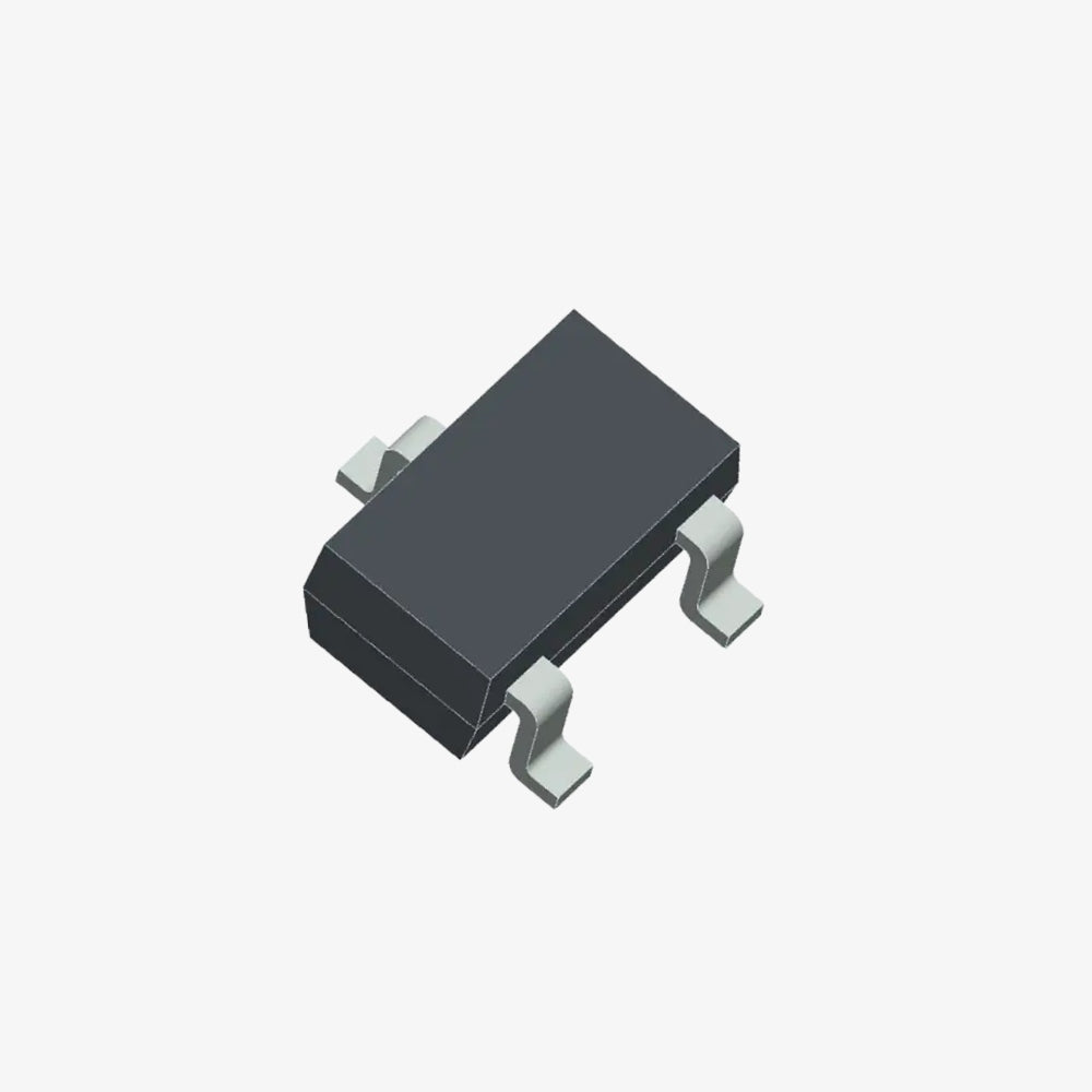
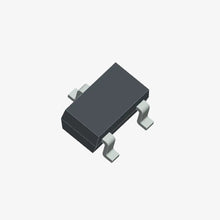
The BSS138LT1G is an N-channel MOSFET designed for low-voltage, low-current switching applications. It is housed in a compact SOT-23 surface-mount device (SMD) package, making it ideal for high-density circuit board layouts. Here’s a detailed description of the product:
Key Features:
- Type: N-Channel MOSFET
- Package: SOT-23 (Surface Mount Device)
- Polarity: N-Channel
- Maximum Drain-Source Voltage (Vds): 50V
- Maximum Continuous Drain Current (Id): 220mA
- Maximum Power Dissipation (Pd): 300mW
- Low On-Resistance (Rds(on)): Typically 3.5Ω at Vgs = 10V
- Gate Threshold Voltage (Vgs(th)): 1.3V to 2.3V
Applications:
- Load Switching: Ideal for switching low-voltage loads.
- Signal Amplification: Suitable for signal amplification in various electronic circuits.
- Battery-Powered Applications: Commonly used in battery-powered applications due to its low power consumption.
- Low-Power DC-DC Converters: Can be used in DC-DC converter circuits for efficient power conversion.
Physical Dimensions:
- Length: Approximately 2.92mm
- Width: Approximately 1.3mm
- Height: Approximately 1.1mm
Pin Configuration:
- Pin 1 (Gate): The gate terminal, which controls the transistor’s switching.
- Pin 2 (Source): The source terminal, which is typically connected to the negative side of the load.
- Pin 3 (Drain): The drain terminal, through which the main current flows when the transistor is in the 'on' state.
Electrical Characteristics:
- Vds (Drain-Source Voltage): 50V max
- Vgs (Gate-Source Voltage): ±20V max
- Id (Continuous Drain Current): 220mA max
- Ptot (Total Power Dissipation): 300mW max
- Rds(on) (On-Resistance): 3.5Ω typical at Vgs = 10V
- Qg (Total Gate Charge): 1.2nC typical
- td(on) (Turn-On Delay Time): 10ns typical
- td(off) (Turn-Off Delay Time): 20ns typical
Note: Product images are for illustrative purposes only and may differ from the actual product.
Returns Policy
Due to the type of products we sell, we accept limited returns. Below are the conditions where we can accept a return request.
1. Damaged During Shipment
If you receive a product damaged during shipment, please notify us within the 3 days of you receive the product, supported by the proper pictures and description. Once our support team accept the return, we will provide a replacement or a complete refund including the return shipping cost.2. Wrong Item Shipped
If your item looks different from what is shown in the image on our website, we will take the item back and provide a refund or replacement as per your choice.
Limitation of Returns
We don't accept the returns for the products damanged by improper use of the product. Moreover we don't accept the return, if the ordered product is not fit for any specific application. Please read the product specifications and datasheet before selecting and ordering a product. Returns are accepted only with 3 days from the date of delivery.Shipping
We ship to all over India with free shipping on all prepaid orders above 500. For Cash on Delivery orders INR 80 will be charged for orders below INR 599 and INR 30 will be charged for the orders above 599. Please contact to our support team at support@quartzcomponents.com for any question related to shipping.
Please note that the Minimum Order Value is INR 500 for COD orders.

